Research Topics (Test)
Nanoelectromechanical systems (NEMS)
Nanoelectromechanical systems (NEMS) are an interesting set of devices that can have many applications involving mass and force sensing as well as high quality-factor tunable resonators. We pursue the engineering of such devices utilizing novel materials including Graphene and Chalcogenides.
Key areas:
- Combining graphene and chalcogenides for RF tunable resonators
- Studying and probing extreme nonlinearity in Room Temperature NEMS
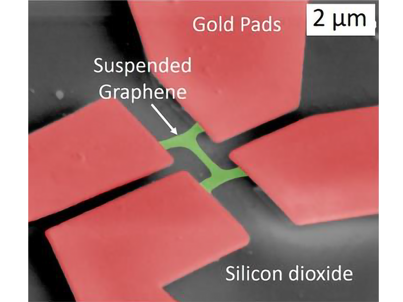
Suspended Graphene NEMS Resonator
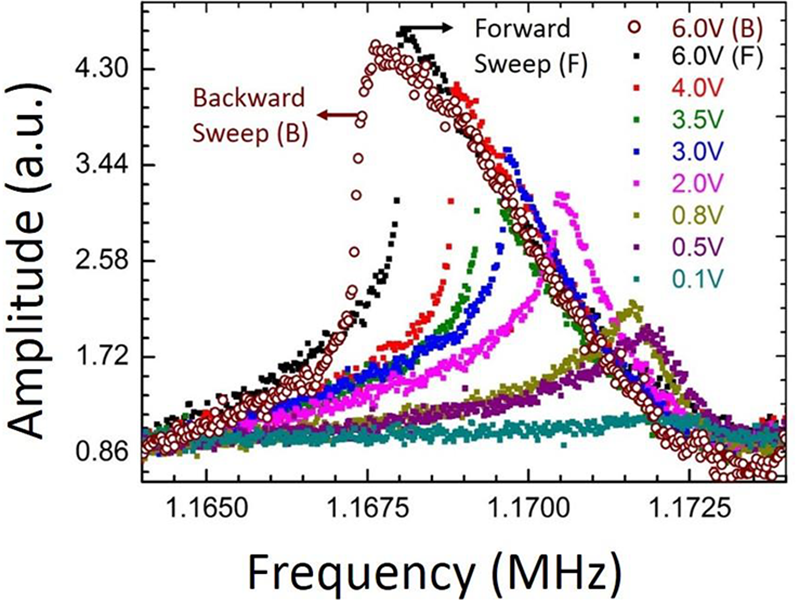
Nonlinearity in NEMS
High-resolution KPM
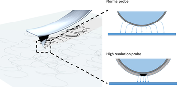
Atomic force microscope (AFM) is a versatile and widely used tool to characterise surface properties at the nanoscale. We mainly use the AFM for topographical and electrical measurements. Our group has invented a modified AFM tip that can achieve electrical resolution that is beyond the geometrical limitations of commercial AFM tips, advancing the field of nanomanufacturing and metrology.
Nanoelectrodes
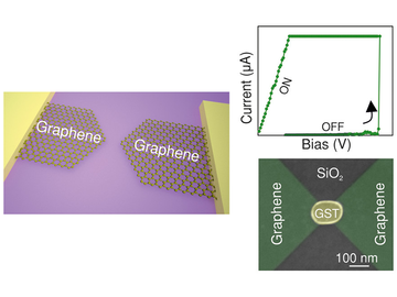
Nanoelectrodes offer to contact nanoscale objects (single molecules and nanocrystals). In our lab, we are utilising nanoelectrodes of graphene to reduce the contact area to these objects in order to avoid undesired gating or screening effect. We further implement those devices with phase-change materials to study the device physics at the nanoscale and thus, we are able to determine the fundamental scaling limits for potential memory-cell applications.
Additive Nanomanufacturing
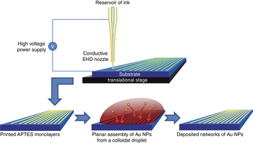
As an additive nanomanufacturing technique, EHD printing exhibits great potential to fabricate flexible electronic and photonic devices with high resolution, good scalability, and low cost. By combining EHD printing with other additive nanomanufacturing techniques such as self-assembly, we have demonstrated that structures with single-particle resolution can be achieved in a cost-effective way.
Probe-based Nanomanufacturing
AFM lithography is a resist-based lithography technique that can achieve high resolution. In contrast with EBL and photolithography that utilise high energy electron beam or photons, it uses AFM tips to image and pattern nanostructures in ambient conditions. This greatly reduces the manufacturing cost. Our goal here is to make this method universal by achieving more complex nanoscale structures not only on silicon-based substrates but also on flexible substrates.
Water-based Nanomanufacturing
With the increasing demand for flexible and wearable technologies, manufacturing techniques to construct advanced devices on flexible substrates are becoming of high importance. Our group focuses on developing effective and sustainable methods to fabricate flexible & functional devices. We achieve it by avoiding the use of organic solvents throughout the fabrication and figuring out ways such as water-only lithography.
Pick-and-place
Nanofabrication techniques are always at the core of creating interesting and useful devices at the nanoscale. In our group, we explore pick-and-place techniques at the nanoscale which opens up many possibilities to create unique devices that could previously only be tested in simulations. Unlike macroscale picking and placing of objects, nano-manipulation has the added complexity of dealing with surface adhesion and chemistry which makes this area of study so challenging yet rewarding and impactful.
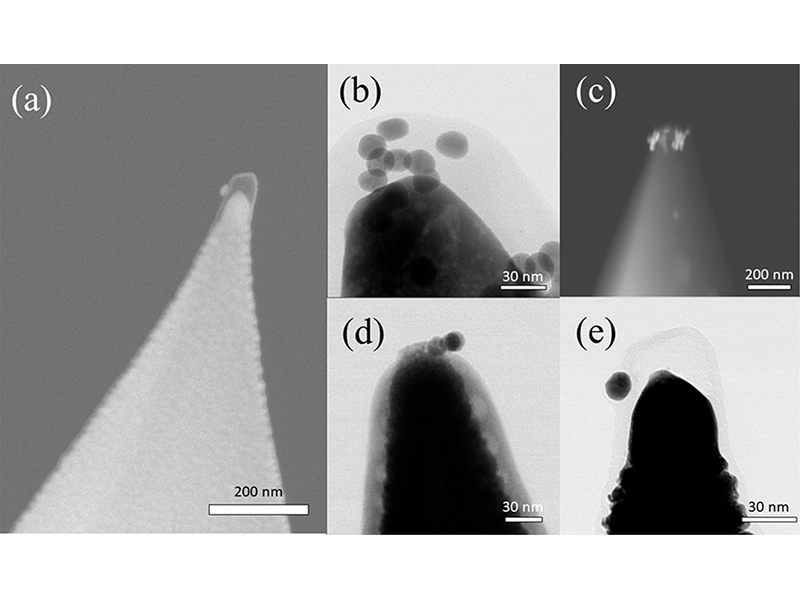
Nanoparticles on an AFM tip
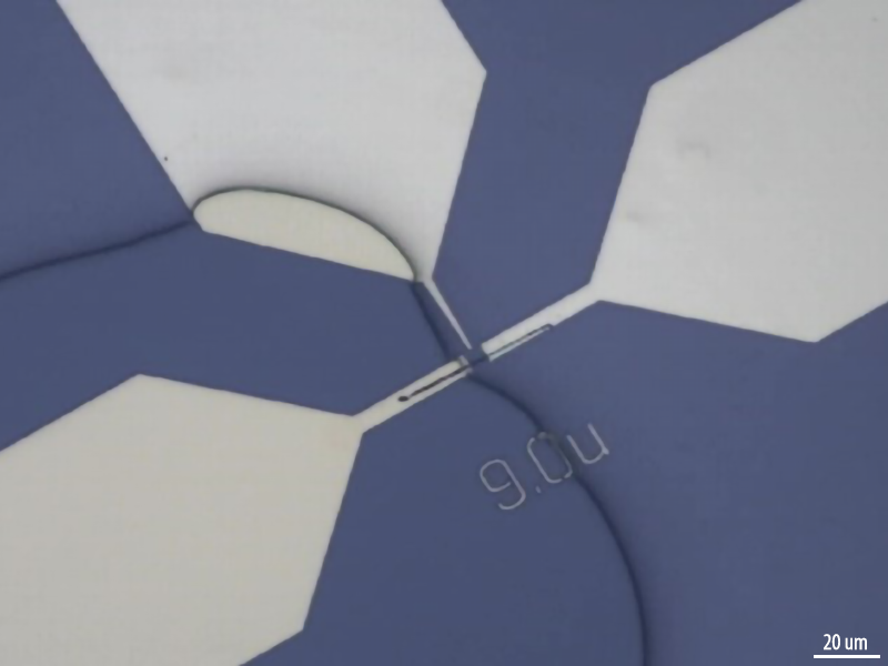
Transferring of a nanowire
Fiber-to-chip Coupling
One of the persistent challenges in photonics is the coupling of light produced by a laser source and guided in a fibreoptic cable from or into a nanoscale device, mainly because of the large mode mismatch between them. A decent coupler should offer low insertion/coupling loss while maintaining a wide bandwidth. Therefore, we aim to advance/develop such techniques to get the optimum performance out of our photonic devices.
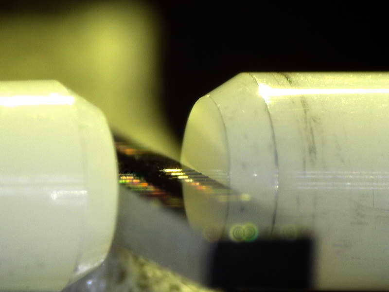
Edge Couplers
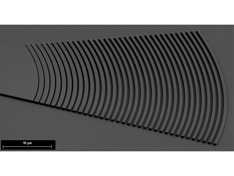
An apodized grating coupler
In-memory Computing
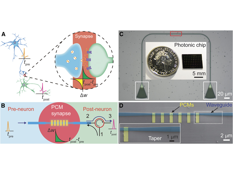
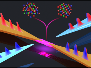
We are now in the age of "big data". To handle such a vast amount of digital information, efforts in improving the performance of computing and storage is coming to an end because of physical limitations. Making use of photonics is a very promising approach to this end. However, we lack the understanding and fabrication know-how of this field because it is still at its relative infancy compared to traditional computing architectures. In 2015, our group has demonstrated, for the first time, a "non-volatile" memory cell using "light" and phase-change materials (PCMs) (click here for details). Keeping the record of storage bits per device and developing different controlling ways recently, we try our best to carry this area forward and pioneer "all-optical" and "neuromorphic" computing.
Optoelectronics of Phase-Change Materials
We create memory devices of phase-change materials (PCM) that can inherently work both in electrical and optical domains, without the need for electrical-to-optical conversion. We overcome the previously-insurmountable size and diffraction limitations by introducing plasmonic platforms.
Reflective Displays and Smart Glazing
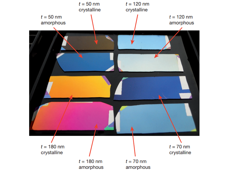
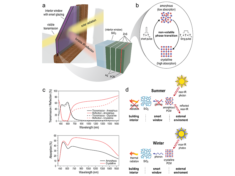
Concerned about the global energy shortage problem, our group engages in environmentally-friendly solutions by offering alternatives based on phase-change materials (PCMs). Reflective displays made of PCMs enable vivid color display without constant power supply, friendly to both eyes and environment unlike LCD and LED/OLED technologies (watch Harish's TEDx talk here). We are also putting our efforts into developing smart windows utilizing PCM thin-films to maintain the indoor temperature of industrial and residential buildings, helping with the energy bills.
Holographic Displays
Holography is simply the spatial phasing of light by means of diffraction & interference, in order to create a three-dimensional (3D) light field. To this end, our group has made a substantial improvement by developing an algorithm for reconstructing the images from the recorded light field. One of our experimental results can be seen below, with the captured "binary image" and the corresponding reconstructed "real image".
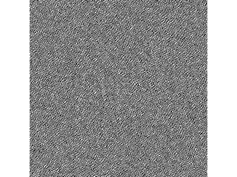
Binary Image

Real Image
We are always experimenting on new areas of research and hold Knowledge Jams to explore new areas. Who knows, one of these may become a major research strand in future!
Ideas in progress:
- Versatile platforms for biodetection
- Investigation of novel phase-change materials


